Youlim Electron Co.,Ltd
Electric & Electronic equipment031-499-2077
PCB Modify Date : 2018-11-24 05:17:39
▣ PCB
Printed Circuit Board (PCB) is also called PWB, and many kinds of parts are pressed together with copper foil on one or both sides of insulation board such as phenol resin and epoxy resin, and then the pattern according to the circuit (wiring) ), And unnecessary parts are corroded to remove copper foil to form a circuit.
The printed circuit board is plated with a hole for connecting the lead of the component or a hole (Via) for connecting the wiring between the top (bottom layer) and the bottom (bottom layer). Apply the top and bottom with Photo Solder Resist (PSR) ink to complete the printed circuit board.
|

|
1. Single side PCB
| 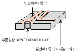 * PCB with circuit formed on one side only, low mounting density and simple manufacturing method * Usage: Used for mass production for public use such as TV, VTR, AUDIO |
| 2. Double side PCB * PCB that is formed on both sides of upper and lower circuits, which enables high density component mounting * The upper and lower patterns are connected by through holes 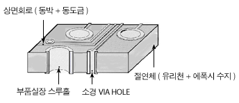
* Application: Mainly used for low function OA equipment such as PRINTER, FAX and low price industrial equipment
|
| 3. Multi Layer Board * This is a three-dimensional PCB with inner and outer circuits, enabling high-density component mounting and shortening of wiring distance in three-dimensional wiring. 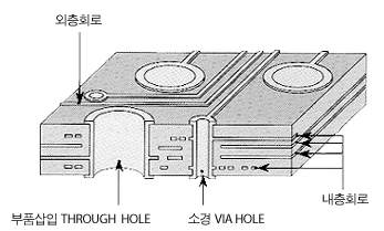 * Application: Mainly used for large computers, PCs, communication equipments, small appliances
|
4. IVH PCB (Interstitial Via Hole MLB)
* Due to the miniaturization of high-performance electronic devices, partial via hole processing is possible to selectively connect circuits to each layer to increase the number of floors and increase the area occupied by the increased wiring amount when designing high density PCB circuits. PCB minimizes the area occupied by holes for circuit connection * Application: Mainly used for high-performance small electronic devices such as mobile phones, notebook PCs, PDAs, etc. |
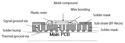
5. BGA PCB (Ball Grid Array PCB)
* As there is a limit to the mounting to existing QFP for the development of package's daffin and fine pitch, it is a new surface mount to replace this. Instead of QFP's LEAD, BARE CHIP is attached to the package SUB board and then the solid ball is attached to the bottom in GRID type. PACKAGE PCB designed to be mounted on MAIN PCB | |
6. R-F PCB (Rigid-Flex PCB)
| 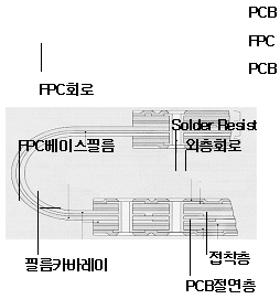  * Due to the high performance miniaturization of electronic devices, a large amount of connection is required between several boards. In order to make the best use of the limited device space and improve connection reliability, the flexible FLEX is integrated between the rigid MLB structures. * Due to the high performance miniaturization of electronic devices, a large amount of connection is required between several boards. In order to make the best use of the limited device space and improve connection reliability, the flexible FLEX is integrated between the rigid MLB structures. |
7. MCM PCB (Multi Chip Module PCB)
| 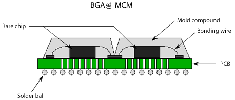 * SINGLE CHIP packaging is limited due to power reduction, IC density, and pin count demand for light and small size reduction of electronic system.Modular CHIP is mounted on a preconfigured board between IC chips. Can be reduced to 1/10 size.
* Application: Mainly used for high performance equipment such as CPU, high performance workstation, notebook PC, ABS, airbag, military radar |
|